中文
中文
 English
第十五期華進論壇邀請函
2018/09/10
為推動我國先進封裝技術水平,促進與業界的合作與交流,華進半導體于2013年2月28日創辦華進論壇。華進論壇每年不定期舉辦,主要邀請國內外知名學者、半導體制造/封裝企業高管、國內外封裝材料/裝備/測試專家,共同就我國先進封裝技術及材料/裝備/測試/質量開展交流與探討,推動我國先進封裝產業的發展。
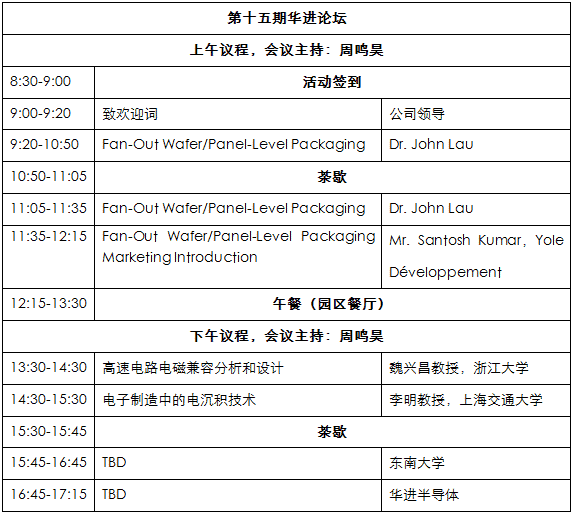
● 地點:華進半導體6樓培訓室(無錫新吳區菱湖大道200號D1棟六樓)
● 議程:
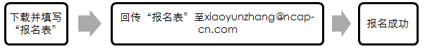
● 報名方式:
方式一:
● 其他事項:
第十五期華進論壇定于本月21日在華進六樓舉辦,活動免費公開,歡迎業界同仁報名參加,具體安排如下:
● 時間:2018年9月21日(周五)8:30-17:15● 地點:華進半導體6樓培訓室(無錫新吳區菱湖大道200號D1棟六樓)
● 議程:
以上為活動初擬議程,根據實際情況調整,請以現場為準!
方式一:
方式二:
通過活動行鏈接報名:http://t.cn/RFgg3pF
報名費用:免費
截止日期:2018年9月18日
華進聯系人:張曉蕓 0510-66679351, xiaoyunzhang@ncap-cn.com
通過活動行鏈接報名:http://t.cn/RFgg3pF
報名費用:免費
截止日期:2018年9月18日
華進聯系人:張曉蕓 0510-66679351, xiaoyunzhang@ncap-cn.com
● 其他事項:
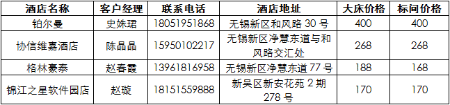
如需住宿,請自行預定酒店,報“華進半導體”享受協議價,費用自理。協議酒店清單如下:
● 附件:
1. 部分嘉賓介紹

1. Fan-Out wafer/Panel-Level Packaging
Biography:
John H. Lau With more than 39 years of R&D and manufacturing experience in semiconductor packaging, he has published more than 470 peer-reviewed papers, 30 issued and pending US patents, and 19 textbooks. John received many awards and is an elected ASME Fellow, IEEE Fellow, and IMAPS Fellow.
Abstract:
The recent advances and trends of the following topics will be discussed. All the information is in the past 3 years.
CONTENTS:
(1) Introduction
(2) Fan-out Wafer/Panel-Level Packaging Formations
→ Chip-first (die face-down)
→ Chip-first (die face-up)
→ Chip-last (RDL-first)
(3) RDL Fabrications:
→ Polymer + ECD Cu/Etching
→ Photosensitive Polymer + ECD Cu/Etching
→ PECVD + Cu-damascene/CMP
→ Hybrid RDLs
(4) TSMC InFO-WLP and InFO-PoP
(5) Samsung FO-PLP and FO-WLP
(6) Temporary Carriers: Wafer vs. Panel
(7) Notes on Dielectric, EMC, and Compression Molding
(8) Examples:
→ Amkor''s SWIFT
→ Amkor''s SLIM with FOWLP
→ SPIL''s FOWLP with Hybrid RDLs
→ STATS ChipPac’s FOWLP PoP for Application Processor
→ STATS ChipPac''s FOFC eWLB
→ ASE''s FOCoS
→ TSMC’s 3D Stacking with FOWLP
→ IMEC’s 3D Stacking with FOWLP and Bridge
(9) 3D IC Heterogeneous Integration and SiP with FOWLP
(10) FOW/PLP Trends
2. Fan-Out Wafer/Panel-Level Packaging Marketing Introduction
Biography:
Santosh Kumar is currently working as Director Packaging, Assembly & Substrates, within the Semiconductor & Software division at Yole Développement (Yole). He worked as senior R&D engineer at MK Electron Co. Ltd where he was engaged in the electronics packaging materials development and technical marketing. His main interest areas are advanced electronic packaging materials and technology including TSV and 3D packaging, modeling and simulation, reliability and material characterization, wire bonding and novel solder materials and process etc. He received the bachelor and master degree in engineering from the Indian Institute of Technology (IIT), Roorkee and University of Seoul respectively. He has published more than 20 papers in peer reviewed journals and has obtained 2 patents. He has presented and given talks at numerous conferences and technical symposiums related to advanced microelectronics packaging.
3. 高速電路電磁兼容分析和設計
個人介紹:
魏興昌,教育部新世紀優秀人才,浙江大學信息與電子工程學院教授,IEEE Senior Member。研究領域為電磁兼容分析、測試以及電磁算法研發。由于在微波混響室方面的研究成果獲得新加坡工程協會頒發的“2007年度卓越工程成就獎”。發表一本英文專著(Modeling and Design of Electromagnetic Compatibility for High-Speed Printed Circuit Boards and Packaging. CRC Press, 2017.)和30多篇IEEE Transactions 論文,曾擔任2010年(新加坡)IEEE Electrical Design of Advanced Packaging and Systems技術程序委員會共同主席(TPC Co-Chair)、2012年、2018年(新加坡)IEEE Asia-Pacific International Symposium on Electromagnetic Compatibility程序委員會主席(Program Chair)和技術論文共同主席(Technical Paper Co-Chairs)等,以及多個國際電磁兼容會議的技術程序委員會委員(TPC Member),并組織多次國際會議Special Session,指導學生獲得多個國際會議學生論文獎。
摘要:
自動駕駛、高性能計算、5G通信、人工智能等,使得高速、高密電子設備全方位滲透入軍事、生產與生活。相關電路的工作頻率不斷刷新,其高次諧波已達數百GHz,導致元器件尺寸與電磁波長相比擬。這些使得PCB板級、封裝級和芯片級的電磁環境變得十分復雜,有害電磁耦合和輻射十分嚴重。因此,電磁兼容分析和設計成為高速電路設計中最具有挑戰性的部分。
高速電路的電磁兼容問題可以分為信號完整性(Signal Integrity,SI)、電源完整性(Power Integrity,PI)和電磁干擾(Electromagnetic Interference,EMI)。本報告重點介紹本團隊在這三個問題上積累的研究成果,包括:
1. 封裝級信號和電源完整性
從電磁理論出發,研發了硅通孔陣列的散射矩陣電磁建模方法;封裝基板的網格狀電源配送網絡的電磁建模方法。
2. 近場電磁掃描
近場電磁掃描成為目前企業界分析其產品電磁干擾的主要工具,將介紹近場掃描技術在電磁干擾診斷中的最新研究結果,重點討論基于近場掃描的噪聲源建模技術。
本報告從電磁場的角度,深入分析高速電路各種電磁干擾背后的電場和磁場原因,并探究解決方案。企業界對高速電路的電磁兼容分析和設計一直有很強的需求,本報告內容主要基于和企業多年合作的研究結果。
4. TBD
個人介紹:
孫鵬博士,華進半導體封裝先導技術研發中心有限公司技術總監、技術導入部部長。2004-2007年瑞典查爾姆斯理工大學攻讀博士學位。畢業后加入香港應用科技研究院(ASTRI)擔任高級工程師,2010年加入星科金朋(STATSChipPAC)擔任主任工程師,經理。2012年加入華進半導體封裝先導技術研發中心有限公司,現主要負責客戶新產品的設計、制造和量產導入工作,已面向產業鏈上下游十余家客戶,包括中國前十大IC設計公司,取得了良好的社會效益和經濟效益。并參與科技部的國家科技重大專項,擔任《高密度三維系統集成技術開發與產業化-關鍵共性技術開發與平臺建設》課題組長,負責單項工藝開發與成套工藝建立,打通WLCSP、Bumping、FCCSP封裝等成套工藝,并實現了穩定的小批量量產服務。在國內外期刊、會議以第一作者/通訊作者身份已發表論文20篇,其中已被SCI,EI檢索10篇以上。獲得美國授權發明專利3項,中國授權發明專利25項;參編譯著《無鉛焊料互聯及可靠性》一本。
 蘇公網安備 32021402001899號